[Blog] Unlocking Edge Connectivity with FPGAs
Posted 12/05/2025 by Lattice Semiconductor
Interest in edge computing has surged as organizations across industries seek smarter ways to automate processes, enhance productivity, and optimize labor. By processing data closer to its source, edge systems can provide benefits like reduced transmission and storage costs and strengthened security. They can also enable the development of advanced machines and devices, from autonomous mobile robots (AMRs) and humanoids to smart medical devices, which can operate with precision and speed.
These advantages are especially important for optimizing production quality and efficiency, and in high-risk and critical infrastructure environments, where real-time monitoring, rapid decision-making, and the capacity to scale can make the difference between success and catastrophic failure. Building devices that meet this demand, however, is anything but simple.
That’s where Lattice's edge AI sensor bridge solution comes in. Purpose-built to streamline the development and deployment of edge systems, this solution combines the strengths of Lattice’s Field Programmable Gate Array (FPGA) components and NVIDIA Holoscan technologies to deliver low latency, high-throughput connectivity for next-generation intelligent edge computing capabilities.
The Challenges Inhibiting Edge Connectivity
Edge developers are forced to operate in incredibly constrained environments. With limited available physical space, power, and compute capacity, the edge is not always the most hospitable setting for high-powered processing capabilities, let alone fully automated systems.
This is a persistent problem for developers. Even as today’s semiconductors are manufactured with advanced processing nodes to enable significantly higher compute power, they are still limited by space and connectivity constraints. The inclusion of these advanced nodes limits the chips’ input/output (I/O) capacity, making system design inherently more complex – especially when these devices need to integrate a wide range of sensor and device input.
What’s more, system requirements are far from static in our modern age. As solutions like artificial intelligence (AI) and machine learning (ML) models continue to evolve, the resources they need, and the speed at which they need them, change as well. Compute needs continue to rise while battery and thermal limitations remain largely the same, creating a difficult and paradoxical scenario for developers.
The Combined Power of FPGAs and NVIDIA Holoscan
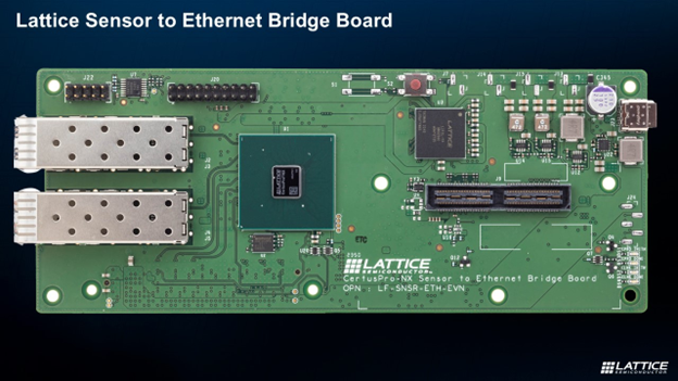
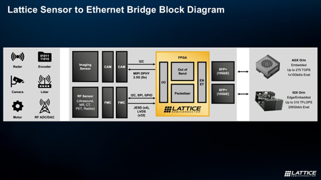
To overcome these constraints, developers need a solution that pairs flexibility with high-performance connectivity. By combining the power of Lattice FPGAs and NVIDIA Holoscan software, developers can create a foundation that supports the rapid development of connected edge applications. The jointly developed sensor to Ethernet bridge board design couples the programmability of a general-purpose Lattice CertusPro™-NX FPGA with the processing power of Holoscan to support seamless sensor fusion at the edge.
Key benefits of this solution include:
- Low latency, high throughput, and scalable sensor streaming.
- A full stack solution that streams sensor data directly into Nvidia’s local memory.
- Ready-to-use open-source software.
- Internal AXI stream and APB control bus enable modular, configurable sensor configuration and streaming.
- Support for up to 2X 10G Ethernet channels.
The solution’s benefits and utility stem from its FPGA-based architecture. By acting as an intelligent bridge between the NVIDIA IGX Thor and AGX Orin hardware components, the FPGA is able to offload high-volume processing tasks from central compute. Lattice FPGAs are especially well-suited for this role due to their low power, deterministic parallel processing capacity, I/O scalability, and built-in security features. This enables them to efficiently pre-process sensor data, while simultaneously reducing overall system power and latency, and freeing up compute resources in central compute for more complex AI models.
The Impact of Streamlined Edge Operations
Together, these powerful technologies help simplify and accelerate the deployment of intelligent edge systems in a variety of settings, while addressing the most pressing challenges edge AI developers face.
To balance growing compute needs with capable I/O support, this FPGA-based solution packetizes all sensor and input data and streams them over Ethernet. This approach leverages Ethernet ubiquity, cost-effectiveness, and high bandwidth, enabling efficient data transfer without monopolizing space. Using this design, FPGAs can support the bridging of legacy I/O capabilities with new requirements, aggregating and packetizing all data and simplifying its transmission from sensor to processor.
The solution also supports inevitable updates required to meet evolving system demands. To meet evolving system needs, FPGAs support low power computer vision and AI processing, reducing link bandwidth and power, while offloading these tasks from central compute. As the system changes and new tasks and workloads are introduced, FPGAs can be reprogrammed, as needed, to maintain the most effective balance of processing duties.
Building Smarter, Faster, and More Scalable Edge Systems
As edge solutions continue to transform industries, the ability to aggregate and process sensor data efficiently and securely at the source is critical. By combining the adaptability of Lattice FPGAs with the capabilities of NVIDIA Holoscan to form a sensor bridge solution, developers can overcome common constraints and accelerate successful edge deployments.
To learn more about the sensor bridge solution, attend this free course from Lattice Insights and register for our upcoming Holoscan webinar with NVIDIA. To dig deeper into how Lattice’s edge AI FPGA solutions can help you build smarter edge applications, contact us today.